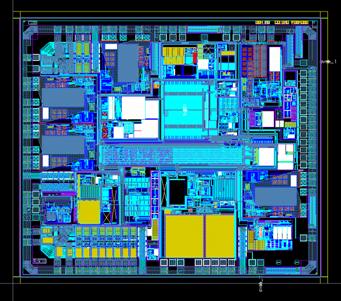
Layout Design
GEDEC is able to provide a full service physical layout design.
Our expertise is mainly focused on full custom design for analog application, power management layout design for power dissipation optimization, substrate isolation, cell reuse and testability.
GEDEC layout experiences come from different technologies, as:
- ATMEL Standard – High Voltage CMOS 0.18/0.35 µm
- ATMEL Embedded Non Volatile Memory
- ST Standard CMOS 0.18/0.35 µm
- ST BCD 0.18/0.35 µm
- Infineon CMOS 0.13/0.35 µm
- XFAB CMOS 0.18/0.35 µm
- TSMC CMOS 0.18 µm
- TSMC BCD 0.25 µm
- UMC CMOS 90 nm
GEDEC layout expertise mainly focused on:
- Full custom design for analog application
- Power management layout design for multi power
distribution, power dissipation optimization and substrate isolation - Layout design for cell reuse
- Layout design for debugging strategy and testability
- Porting and shrinking in different technology